Designing a PCB with Eagle CAD tool can be a tough task. Not only does it require knowledge of electronics but learning the jargon takes time. In this tutorial, I will layout the various terminology you should know when trying to make a PCB. Achieving an understanding of such acronyms and terminology will ease communication with other people excited about taking their conceptual electronic circuit to a final board with CAD softwares. Let’s begin.
General Circuit Acronyms
Integrated Circuit (IC)
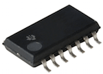
This is the brains of an electronic circuit. In most cases, you will use some sort of IC in your design. As an example, a microcontroller is an IC. You will purchase ICs through stores, such as Sparkfun.com. If your design requires computation and/or an interface to a computer, you will use a microcontroller and in this case, you may resort to an Arduino due to its easy-of-use. Figure 1 shows a typical IC.
SMD
This stands for Surface Mount Device. These are the small electronic parts (resistors, capacitors, among others). In general, these are not your typical devices used in breadboards or for testing. They are usually used on PCBs. They have a small footprint to save space.

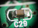
There are various sizes of typical SMD technology. They range from 0402, 0603, 0805, 1210, and more. The 0402 SMD parts are smaller than the 1210. The large components (1210) take more space on your PCB. Therefore, depending on the size of the PCB and your design, you can use smaller or bigger size. However, do note that the smaller sizes are more difficult to solder.
GND
This refers to ground. A GND is necessary in circuit. It is the reference at 0 volts. Therefore, all other voltages in the circuit are relative to GND.
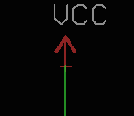
VCC/Vin
This refers to the input voltage from an external source. The input voltage can be obtained from AC power outlets, batteries, or even solar panels. In general, anything that can supply power to the circuit. VCC is relative to GND. You can see an example of VCC in the below image.
PCB Schematic Terminology
Net
This is a virtual representation of a wire. In the real-world, you would use wires to make connections between different components and ICs. On PCBs, wires are never used instead a copper route is created on the PCB board. Such a route is represented in the softwares by nets.
Pin
This is a connection point in an IC or component. For example, a resistor has two sides which can be seen as two pins. An IC can have as low as 3 pins to as many as 128 pins and beyond. As a designer, you will add net connections to these pins. In Figure 3, the VCC component has a one pin, which needs a connection.
Electric Rule Check (ERC)
After creating a schematic, you will run the ERC check. This will make sure you follow the basic rules of electronics. It will generate errors, if for example, you connect VCC and GND together. It will also give warnings (not errors) if some of the pins on ICs, for example, do not have connections.
PCB Board Terminology
Wire
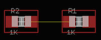
After creating the schematic, you can now transfer that over to create the PCB board. Each net created in the schematic now has a corresponding wire in the PCB board layout. This is a visualization tool to show you that a physical copper connection must exist, otherwise your circuit will not perform as designed. This wire can be see in Figure 4 in yellow color. The items R1 and R2 are PCB representation of resistors (0402 size).
Route
Using the wires as a visualization, you can route those connections. A route is made of copper when the PCB is being manufacture.
Vias

A via is a physical hole (with conductive copper) on the PCB board. If you are attempting to create a compact PCB, then the routing may touch either SMD components or other routes. This cannot happen because then you are mixing signals, e.g. VCC and GND cannot touch. Thus, you can create a via which connects to a wire. This via then goes to a second layer on the board (we will deal with only 2 layers representing the top and bottom of the physical board). This second layer will be the bottom of the board where there may be no or a few SMDs, e.g. resistors. This technique gives you more room to work with. I will get into much more detail regarding vias with video tutorials.
Layers
In these tutorials, I will deal with 2 layers for simplicity. Note that in most designs, 2 layers are enough. In this case, the two layers are referred to as the top and bottom, and correspond to the two sides of the PCB. Copper routes can be created on both layers.
Design Rules Check (DRC)
Similar to the ERC in Schematics, the DRC is the final check before being sent to be fabricated. The DRC ensures your design meets the standards set forth by the fabricator. This check includes verifying the physical size of the board, width of routes, diameter of vias, number of layers, distance from the edge of the boards to the nearest SMDs, and much more. The DRC check can be a life-save since without it, you would have no way of knowing if the PCB will turn out as planned. Most of the time the fabricators will provide a DRC file for you to use. You will then run your design through the DRC file to see if it everything works as planned. I will get into much more detail on this.
Final Thoughts
I have laid out the acronyms and definitions you will need to succeed in creating your first PCB. Of course, there are many more definitions. If you would like to see a list of all definitions, refer to the glossary. However, these mentioned jargons are enough to begin learning PCB design.
Did you have any difficulties with this tutorial? Please share your thoughts and/or difficulties by leaving a comment below.
Comments
One response to “Definitions and Acronyms Used – PCB Design Tutorial”
[…] the procedure to create a new library. Finally, I will show you how to design a symbol using a SMD resistor as an […]